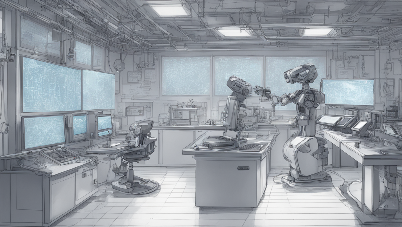
Researchers from MIT and the Chinese University of Hong Kong have made a groundbreaking breakthrough in electronics manufacturing with the development of neural lithography, an advanced AI technique. The researchers have successfully leveraged machine learning to simulate the complex process of photolithography, a crucial step in the production of computer chips and optical devices. By bridging the gap between design intentions and real-world manufacturing outcomes, this innovation promises to revolutionize the industry.
Photolithography, which involves the use of light to etch precise features onto surfaces, often encounters deviations during the manufacturing process, leading to suboptimal device performance. To address this challenge, the researchers utilized actual data from the photolithography technology to develop a digital simulator that accurately replicates the fabrication process. By faithfully simulating the way the system realizes a design, this simulator significantly enhances accuracy and efficiency in electronics manufacturing.
Cheng Zheng, a mechanical engineering graduate student and co-lead author of the research paper, acknowledges the difficulties in coordinating software and hardware to construct a high-fidelity dataset. He explains that while the idea of using real data may seem simple, its execution is complex and expensive. However, the team’s extensive exploration and risk-taking paid off, as they discovered that real data outperformed simulators based on analytical equations. The researchers have demonstrated that despite the challenges and costs involved, utilizing real data is not only more efficient but also more accurate.
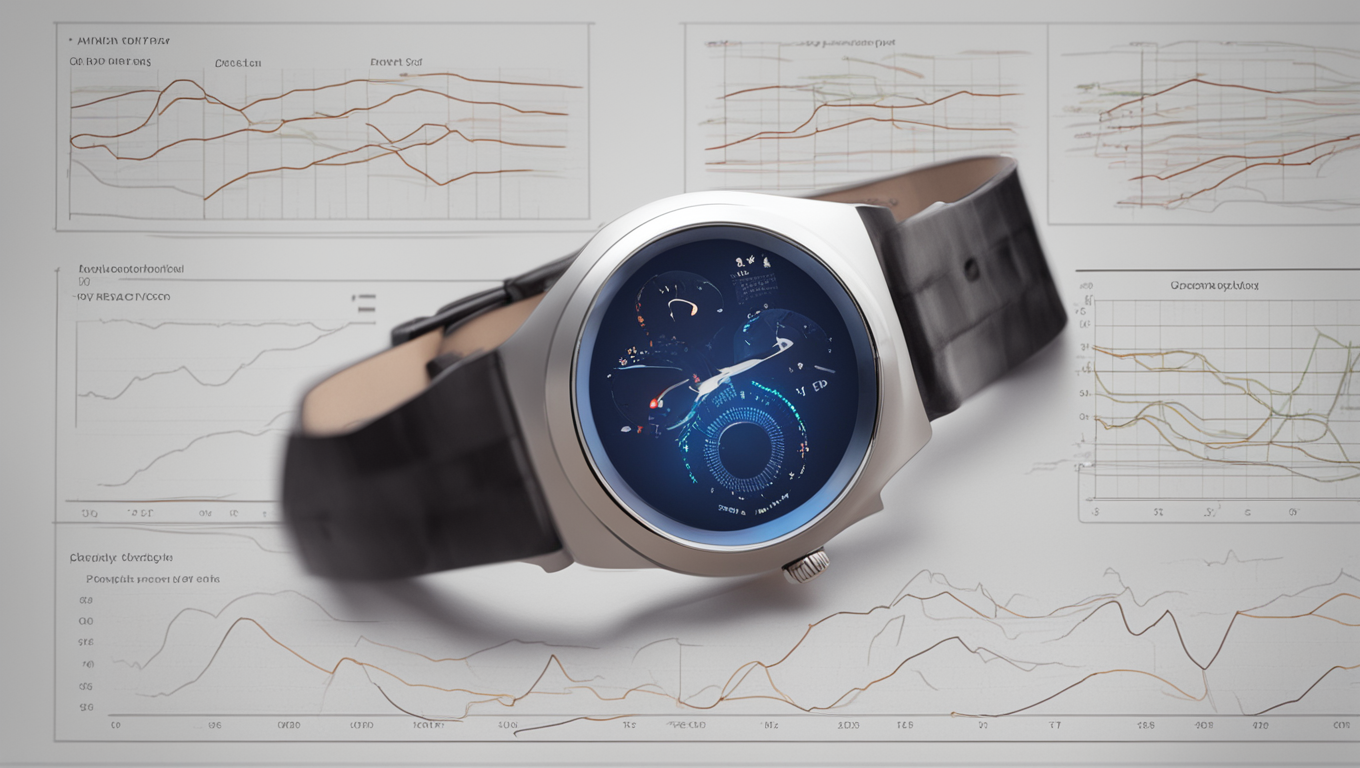
The application of neural lithography goes beyond improving photolithography itself. By integrating the photolithography simulator with another simulator that simulates device performance in downstream processes, the researchers have created a full design framework. This combined simulation technique allows users to develop optical devices that precisely match their design specifications, leading to improved overall task performance. A wide range of applications in various industries such as mobile cameras, augmented reality, medical imaging, entertainment, and telecommunications are anticipated for this groundbreaking technology.
The potential impact of this research is significant. With the neural lithography simulator, fabricated objects can achieve the best possible performance in downstream tasks. This is particularly promising for technology such as computational cameras, which have the potential to revolutionize future camera capabilities by making them more powerful and miniaturized. The researchers found that even with post-calibration techniques to improve results, the performance still did not match that achieved with their photolithography model. This underscores the superiority of their simulator and its potential impact on the industry.
Looking ahead, the MIT researchers plan to further enhance their algorithms to accommodate more complex devices and conduct tests with consumer cameras. They also aim to expand the approach to include different types of photolithography systems, including those that utilize deep or extreme ultraviolet light. By presenting their research at the SIGGRAPH Asia Conference, the researchers have introduced a paradigm shift in the integration of AI and manufacturing processes. This breakthrough sets the stage for more accurate and efficient production of optical devices, paving the way for further advancements in the industry.


Use the share button below if you liked it.