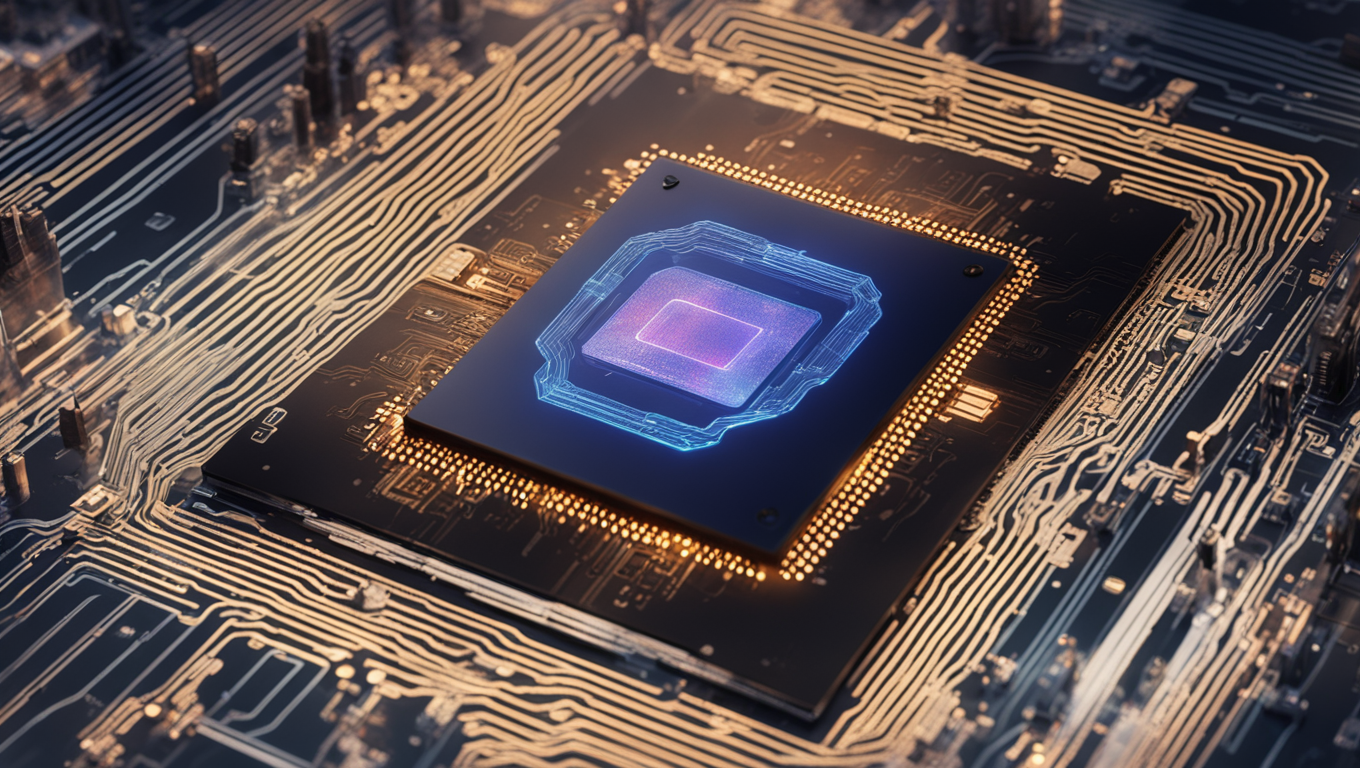
Samsung Electronics has just made a groundbreaking announcement in the artificial intelligence (AI) chip market. The company has revealed the development of HBM3E 12H, the industry’s first 12-stack HBM3E DRAM and the highest-capacity HBM product to date. This new memory chip is set to revolutionize AI applications and address the growing demand for higher capacity HBM in the industry.
The HBM3E 12H is a memory chip that offers low power consumption and wide communication lanes. It utilizes vertically stacked memory chips to overcome the processing bottlenecks faced by conventional memory chips. With the exponential growth of the AI market, the advanced and high-capacity HBM3E 12H will serve as the optimal solution for future systems that require more memory.
Bae Yong-cheol, Executive Vice President of Memory Product Planning at Samsung Electronics, commented on the new memory solution, stating, “The industry’s AI service providers are increasingly requiring HBM with higher capacity, and our new HBM3E 12H product has been designed to answer that need. This new memory solution forms part of our drive toward developing core technologies for high-stack HBM and providing technological leadership for the high-capacity HBM market in the AI era.”
The HBM3E 12H offers a record-breaking bandwidth of up to 1,280 gigabytes per second (GB/s) and an industry-leading capacity of 36 GB. These figures represent more than a 50 percent improvement compared to the previous 8-stack HBM3 8H. The chip also features advanced thermal compression non-conductive film (TC NCF) technology, ensuring that the height specification of the 12-layer products remains the same as the 8-layer ones. This technology offers added benefits, especially for higher stacks, and helps mitigate chip die warping.
Samsung’s HBM3E 12H is expected to significantly enhance AI training speed and increase the number of simultaneous users of inference services. In comparison to adopting HBM3 8H, the average speed for AI training can be increased by 34 percent, and the number of simultaneous users can be expanded by more than 11.5 times. Furthermore, the enhanced performance and capacity of the HBM3E 12H will allow customers to manage their resources more flexibly and reduce the total cost of ownership for data centers.
The announcement from Samsung comes amidst fierce competition in the HBM market. Micron Technology, a US-based chipmaker, has already begun mass production of HBM3E, surpassing Samsung and SK hynix. Micron’s latest chip, with a capacity of 24 GB, will be integrated into Nvidia’s H200 Tensor Core GPUs. The HBM market, which only accounted for 1 percent of the total memory chip market in volume last year, is predicted to more than double this year.
With Samsung and SK hynix both vying for market dominance, each currently holding a 45 percent market share, the introduction of Samsung’s HBM3E 12H could potentially shift the balance in the industry. Micron, with around 10 percent of the market share, also poses a significant challenge.
Samsung’s technological breakthrough demonstrates its commitment to innovation and technological leadership in the AI era. The HBM3E 12H is the product of extensive research and development, which will pave the way for more advanced AI applications and contribute to the growth and development of the AI industry as a whole.


Use the share button below if you liked it.